- Tel.: +49 (0)89 37156018-0
- info@vertilas.com
InP BTJ VCSEL Device Concept
Indium Phosphide (InP) Vertical Cavity Surface Emitting Laser Diode (VCSEL)
Vertilas lasers are based on a VCSEL concept. This laser device consists of vertically stacked layers (Fig. 1) and the laser beam is emitted vertically to the surface of the semiconductor device. In comparison, edge emitting lasers, such as distributed feedback lasers (DFB), feature a laser structure parallel to the surface of the device and emit the light from the edge of the laser chip.
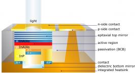
Vertilas has pioneered the development of InP based long wavelength (lw) VCSELs. This laser design features a dielectric bottom mirror, a buried tunnel junction for the current confinement, a gold substrate acting as a heat sink, a multi quantum well (MQW) active region and an optimized waveguide design.
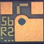
Fig. 1: Cross section of an InP VCSEL Fig. 2: InP VCSEL top view
This VCSEL concept has an optimised thermal design that allows laser operation from -20°C to +80°C, some product variants allow an even wider temperature range from -40°C to +90°C. The lasers have a an excellent single mode performance with a side mode suppression ratio of 40 dB and more. The laser device is very efficient and consumes typ. only 10 mW to 20 mW in electrical power. The optical power reaches up to 5 mW, depending on operating conditions and the laser version.The material structure consists of III-V semiconductors, such as In, P, Al, As and Ga and enables the production of lasers from 1.3 µm to 2.3 µm.
The essential VCSEL properties are:
- Low current threshold and power consumption
- Single-mode operation
- High efficiency
- Circular optical beam
- Cost-effeicient fabrication and testing capability
- 1D and 2D VCSEL arrays